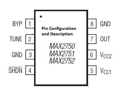
MAX2750 Monolithic VCO Pin Description and Datasheet
MAX2750 Monolithic VCO Pin Description and Datasheet - You will be provided with a pin description and configuration of MAX2750 Voltage-Controlled Osc

This monolithic VCO device used to be applied in 802.11b DSSS WLAN, 802.11 FHSS WLAN Home RF, and 2.4GHz Bluetooth ISM Proprietary Radio.
According to the MAX2750 series datasheet, each IC combines a fully integrated oscillator and output buffer in a miniature 8-pin uMAX package. And below, you will see its pin description:
- VCO Bypass.
- Oscillator Frequency Tuning Voltage Input.
- Ground Connection for Oscillator and Biasing.
- Shutdown Logic Input.
- Bias and Oscillator DC Supply Voltage Connection.
- Output Buffer DC Supply Voltage Connection.
- Buffered Oscillator Output.
- Ground Connection for Output Buffer.
You may see full MAX2750 datasheet here in pdf.
Tags: MAX2750 series circuit, voltage controlled oscillator, MAX2750 pin, monolithic VCO, VCO device,
Copyright www.unboxing.eu.org
